A computer is a machine that takes in information, works on that information by following instructions, and gives back a result. That is how computers work at every level: take in data (input), process the data with the CPU, hold the data in memory and storage (store), and send out the result (output). Everything a computer does, from opening a photo to playing a game, is built from this one cycle running billions of times a second on tiny on-off switches. This article explains each step of the cycle, the parts that carry it out, and how software reaches the hardware.
The Four Steps: How a Computer Works in Plain English
Every computer follows the same four-step cycle: input, process, store, and output. The cycle repeats for as long as the machine is switched on, and the four steps below are the big picture before any of the parts:
- Input. You give the computer data using a keyboard, mouse, microphone, or touchscreen. The device turns your action into digital data (1s and 0s).
- Process. The CPU (the processor) follows instructions to work on that data , doing the math, comparisons, and decisions.
- Store. RAM holds what the computer is working on right now, while a drive (SSD or hard drive) keeps your files for the long term.
- Output. The computer sends the finished result to a screen, speakers, or printer so you can see or hear it.
The scale has changed far more than the routine. Encyclopaedia Britannica records that ENIAC, the first general-purpose electronic computer, ran on 17,468 vacuum tubes and completed about 5,000 additions per second in 1946. A current desktop processor completes billions of instructions per second, yet the loop of input, process, store, and output has stayed exactly the same.
What Are the Main Parts of a Computer?
A computer is built from a handful of core parts, each handling one job in the cycle. They all plug into the motherboard so they can talk to each other:
CPU (Processor)
RAM (Memory)
Storage (SSD / HDD)
Motherboard
Input devices
Output devices
Together these parts are the hardware. Each part gets a fuller breakdown in the computer hardware guide.
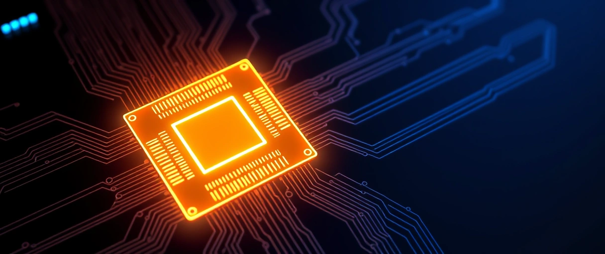
How Does the CPU Process Instructions?
The CPU works by repeating a tiny three-step loop called the fetch-decode-execute cycle, once for every single instruction. This loop is the real engine of a computer:

- Fetch. The CPU grabs the next instruction from memory. A counter inside the CPU keeps track of which instruction is next.
- Decode. The control unit reads the instruction and works out what it means , add two numbers, move some data, or make a decision.
- Execute. The CPU carries out the instruction, then saves the result. Then it loops straight back to fetch the next one.
A clock inside the CPU sets the pace for the loop. Intel’s ARK database lists the Core i9-14900K at a 3.2 GHz base frequency and a 6.0 GHz maximum turbo frequency, so its fastest cores can start this cycle up to 6 billion times each second. That tick rate is the clock speed, measured in gigahertz (GHz).
Why Do Computers Use Binary (1s and 0s)?
Computers use binary, only 1s and 0s, because their building blocks are tiny switches that are either on or off. The switch is a transistor. A transistor either lets electricity through, which the computer reads as 1, or blocks the current, which reads as 0. Chip makers now fit tens of billions of these switches onto one piece of silicon; Apple’s October 2023 announcement of the M3 chip family lists the M3 Max at 92 billion transistors on a 3-nanometer process.
A single 1 or 0 is called a bit. Strings of bits build up into numbers, letters, colours, sounds, and images. Two states also keep the machine dependable, because on or off is hard to confuse. Reading ten separate voltage levels would invite constant errors; reading two almost never does.


How Do Memory and Storage Work Together?
Memory (RAM) and storage (a drive) are both for holding data, but they do very different jobs. The difference comes down to speed and whether they remember after power-off:
RAM: working memory
Storage: the drive
RAM is fast but forgetful, so the computer copies what it needs from the drive into RAM, works on it there, and writes the changes back to the drive. Close an app without saving and the work is gone, because the work existed only in RAM. Save the file, and the drive keeps a permanent copy. Both parts plug into the motherboard, which carries data between them and the CPU.
Our recommendation for anyone buying or upgrading a computer is to make an SSD the main drive. Moving from a mechanical hard drive to an SSD shortens boot times and app loading more than most other single upgrades.
What Does the Operating System Do?
The operating system (OS) is the master software, such as Windows, macOS, or Linux, that runs the whole computer and lets your apps use the hardware. The OS shares the CPU by giving each open app a turn on the processor, switching between them faster than a person can notice. The OS also decides what sits in RAM, keeps files organised on the drive, and stops one app from interfering with another. To control the hardware itself, the OS uses small programs called drivers: one for the screen, one for the keyboard, one for the printer or network adapter.
How Does Data Flow from a Keypress to the Screen?
When you press a key, the data travels a clear path through the computer before it shows up on screen. It is the full input -> process -> output cycle in action:
- You press a key. The keyboard turns that press into a digital signal and sends it to the computer.
- The OS receives it. A driver and the operating system work out which key you pressed and which app should get it.
- The app reacts. The active app (say a word processor) takes the keypress and updates what it is doing , adding the letter you typed.
- The CPU and memory work. The processor figures out the new picture for the screen and holds it in memory.
- The screen updates. The graphics hardware sends the finished image to your monitor, and you see the letter appear , all in a fraction of a second.
How Does Software Turn into Something the Computer Can Run?
Programs are written by people in a readable language, then translated down into the 1s and 0s the CPU understands. Programmers write code in languages such as Python, Java, or C++, using words and symbols a human can read. A compiler (or an interpreter) then converts that readable code into binary machine instructions for the CPU. Those instructions enter the fetch-decode-execute loop and become real actions: switches flipping on and off. Every app you use is a long list of simple instructions, translated into binary and fed through the CPU’s loop one after another.
A Quick Look Inside a Real CPU
The same fetch-decode-execute idea scales up inside modern processors, which run several instructions at once to go faster. You do not need the details to understand a computer, but here is the bridge to the real hardware:

Pipelining lets the CPU work on several instructions at different stages at the same time instead of finishing one before starting the next. Multiple cores take the idea further: each core is a complete processor on the same chip, so separate tasks run truly in parallel. Caches, small pools of high-speed memory inside the CPU, keep frequently used data close so the cores wait less on slower RAM.
As of 2026, Intel’s current desktop family is the Core Ultra 200S series, led by the 24-core Core Ultra 9 285K, and AMD’s is the Ryzen 9000 series built on the Zen 5 design, led by the 16-core Ryzen 9 9950X. The example CPUs below all run the same cycle, just at different speeds and core counts:
| CPU | Base Clock | Boost Clock | Cores | L3 Cache |
|---|---|---|---|---|
| Intel Core i9-14900K | 3.2 GHz | 6.0 GHz | 24 (8P+16E) | 36 MB |
| AMD Ryzen 9 7950X | 4.5 GHz | 5.7 GHz | 16 | 64 MB |
| Apple M3 Max | N/A | ~4.05 GHz | 16 (12P+4E) | 48 MB |
| Qualcomm Snapdragon 8 Gen 3 | N/A | 3.3 GHz | 8 (1+3+4) | 12 MB |
When the theCoreiTech team reads a spec sheet like this one, our recommendation is to check core count first, boost clock second, and cache third, then match those numbers to the work the computer will actually do.
What Language Does the CPU Actually Speak?
Each CPU family understands its own set of binary instructions, called its instruction set, which is why an app built for one type of chip may not run on another. Two families dominate today:
x86-64
ARM
This is why a phone app and a desktop program are built differently: they speak to different chip families. The software is translated to match the chip it will run on.
Last Thoughts on How Computers Work
A computer is far simpler at its core than it looks. It runs one repeating cycle (take in data, process it with the CPU, hold it in memory and storage, send out the result) billions of times a second. Underneath every app, photo, and video are just 1s and 0s: tiny switches flipping on and off. The hardware is the machine, the software is the instructions, and the operating system ties them together so the whole thing feels effortless.
Key Takeaways:
- The cycle: every computer runs the same loop: input, process, store, output.
- The CPU is the brain; it repeats a tiny fetch-decode-execute loop for every instruction.
- RAM holds what you are working on now (and forgets at power-off); storage keeps your files for good.
- Everything is binary, 1s and 0s, because chips are made of switches that are either on or off.
- Hardware is the machine, software is the instructions, and the operating system makes them work together.
Frequently Asked Questions (FAQs)
How many instructions does a CPU execute per second?
A modern desktop CPU at 3–5 GHz executes between 3 billion and 20 billion instructions per second depending on instruction mix, core count, and IPC. Multi-core processors multiply this by core count.
What is the role of the control unit in the CPU?
The control unit decodes binary opcodes and generates electrical control signals that direct data movement between registers, activate the ALU, and manage memory read/write operations during each instruction cycle.
Why does RAM lose data when the computer turns off?
DRAM cells store bits as capacitor charges that discharge within milliseconds without refresh cycles. Power-off stops refresh operations, causing all stored charge, and thus all data, to dissipate immediately.
What is the difference between a 32-bit and 64-bit CPU?
A 64-bit CPU uses 64-bit wide registers and supports 64-bit memory addressing, enabling access to over 4 billion times more RAM than 32-bit CPUs (which address a maximum of 4 GB).
How does a CPU execute a conditional branch instruction?
The CPU evaluates condition flags set by a prior comparison instruction. If the condition is true, the Program Counter loads the branch target address. If false, the PC increments to the next sequential instruction.