GPU architecture is the design that defines how a graphics processor organizes its cores, memory, and execution units to render graphics and run parallel computation. Nvidia ships architectures named Ada Lovelace and Blackwell, while AMD ships the RDNA family, each revising core counts, cache, and efficiency over the prior generation.
What Is GPU Architecture?
GPU architecture is the design that defines how a graphics processor arranges its cores, memory, and execution units. It sets the number and grouping of shader cores, the dedicated ray-tracing and AI hardware, the cache and memory layout, and how work is scheduled across the chip to run the parallel workloads in the overview of how GPUs work.
- Two layers: the high-level organization of cores and memory, and the low-level circuit design built on a specific process node.
- Vendor families: Nvidia (Ada Lovelace, Blackwell), AMD (RDNA), and Intel each revise the design every generation for more performance per watt.
- Why it matters: two cards with similar core counts can perform very differently on different architectures, because the design sets the ceiling for what the video memory and shader cores achieve together.
What Are Streaming Multiprocessors and Compute Units?
Streaming multiprocessors (SMs) and compute units (CUs) are the building blocks that group shader cores and shared resources inside a GPU. Nvidia calls its block an SM, AMD calls its a CU, and a chip holds many of them; the scheduler spreads work across all so thousands of cores run in parallel.

- Inside each block: a set of shader cores, a scheduler, a register file, and a slice of L1 cache.
- Nvidia SM (Blackwell): 128 CUDA cores + 1 RT core + 4 Tensor cores.
- AMD CU: 64 Stream Processors + ray accelerators.
- Scaling: a flagship just holds many more blocks than a budget card on the same architecture – core counts scale with the SM count.
The flagship RTX 5090 carries 170 SMs, which is how its core counts add up:
What Is the Difference Between Shader, RT, and Tensor Cores?
Shader, RT, and Tensor cores differ in the type of calculation each unit accelerates – dedicated hardware runs its specific workload far faster than general shader cores would:
| Core Type | Nvidia / AMD Name | Function | Workload |
|---|---|---|---|
| Shader core | CUDA core / Stream Processor | General floating-point and integer math | Vertex and pixel shading, compute |
| RT core | RT core / Ray Accelerator | Ray-triangle intersection and BVH traversal | Ray-traced lighting, reflections, shadows |
| Tensor core | Tensor core / AI Accelerator | Low-precision matrix multiplication | DLSS upscaling, AI training and inference |
Shader cores carry the bulk of rasterized rendering, RT cores activate when ray tracing is enabled, and Tensor cores power DLSS and AI. A modern GPU mixes several core types, each tuned for a different job:
Shader cores
RT cores
Tensor / AI cores
ROPs and TMUs
How Does the GPU Memory Hierarchy Work?
The GPU memory hierarchy works by placing small fast memories near the cores and large slow memory farther away, so frequently used data stays close to the shader cores and they stall less. It runs from registers out to VRAM:
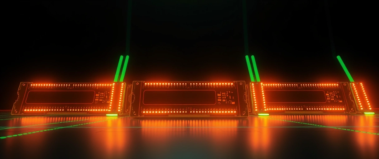
- Registers are the fastest storage, private to each shader core, holding the operands of in-flight calculations.
- L1 cache and shared memory sit inside each streaming multiprocessor, holding data shared among the cores in that block.
- L2 cache is shared across the whole GPU, reducing trips to VRAM; AMD’s Infinity Cache and Nvidia’s large L2 expand this level.
- VRAM is the large GDDR6 or GDDR6X memory on the card, holding textures, frame buffers, and geometry.
Recent architectures enlarge the on-chip caches to cut VRAM traffic, because cache bandwidth far exceeds memory bandwidth. AMD Infinity Cache and Nvidia’s expanded L2 raise effective bandwidth and efficiency without a wider memory bus.
What Are the Recent GPU Architecture Generations?
The recent generations are Nvidia Ada Lovelace and Blackwell, and AMD RDNA 3 and RDNA 4. Each revises core counts, cache sizes, ray-tracing throughput, and process to raise performance per watt:



- Nvidia Ada Lovelace (RTX 40): 3rd-gen RT cores and 4th-gen Tensor cores.
- Nvidia Blackwell (RTX 50): further ray-tracing and AI gains, with GDDR7 memory.
- AMD RDNA 3 (RX 7000): a chiplet design that splits the graphics compute die from memory-cache dies.
- AMD RDNA 4: refined ray tracing and efficiency.
A newer architecture often outperforms an older one at the same core count, so weigh the generation, not just the core count – a factor the graphics card selection guide covers.
How Does the Process Node Affect a GPU?
The process node sets how small and dense the transistors are, which governs efficiency and how many cores fit on a die. Measured in nanometers (5 nm, 4 nm), it names the foundry technology from a maker such as TSMC.
- Smaller node, more cores: denser transistors pack more shader cores into the same area.
- Smaller node, less power: lower energy per transistor switch, so more performance per watt and less heat.
- Current nodes: Ada Lovelace on a custom TSMC 4 nm node; RDNA 3 on a 5 nm graphics die paired with 6 nm cache dies.
A denser node also lowers the heat the GPU cooling system must remove. Process gains account for a large share of each generation’s improvement, alongside the core redesign.
How Does Architecture Affect Efficiency?
Architecture affects efficiency by determining how much performance the GPU delivers per watt. Performance per watt depends on the node, the cache design, the clock-and-voltage curve, and how well the architecture keeps the shader cores busy.
- Bigger on-chip cache (AMD Infinity Cache, Nvidia’s expanded L2) cuts power-hungry trips to VRAM.
- Lower power, less heat: a more efficient card eases the cooling demand and enables quieter or smaller designs.
- Critical for laptops and integrated graphics, where a fixed power budget rewards the most efficient architecture.
Each generation improves efficiency through a newer node, larger caches, and a refined core design together – which is why a new mid-range card can match an older high-end card while drawing less power.
How Does GPU Architecture Differ From CPU Architecture?
GPU and CPU architectures differ in how the chip splits transistors between control logic and arithmetic cores. A CPU spends transistors on control logic, branch prediction, and large caches to finish one sequential task fast; a GPU spends them on thousands of simple cores for parallel throughput.
- Core count: a CPU has dozens of cores and threads; a GPU has thousands of shader cores.
- Memory: a GPU uses a wide, high-bandwidth VRAM bus; a CPU uses lower-bandwidth but lower-latency system memory.
- Workload: a CPU runs branch-heavy serial logic; a GPU runs data-parallel math.
Both architectures share a cache hierarchy and a clock-and-voltage curve, but the balance of resources differs sharply, which is why each processor suits a different kind of work.
How Do GPU Generations Improve Over Time?
GPU generations improve through a denser process node, a redesigned core layout, larger caches, and refined specialized hardware – each generation raises performance per watt, so a new mid-range card can match an older high-end one at lower power. The gains come from several directions:
- Process node shrinks pack more transistors into the same die area, raising core counts and lowering power per operation.
- Core redesigns raise the work each shader core completes per clock and improve how the scheduler keeps the cores busy.
- Larger on-chip caches, such as AMD Infinity Cache and Nvidia’s expanded L2, cut power-hungry trips to VRAM.
- Improved RT and Tensor cores raise ray-tracing and machine-learning throughput, widening the gap in those workloads each generation.
- Higher memory bandwidth from faster GDDR6X and wider buses keeps the growing core count supplied with data.
So weigh the architecture generation alongside core count and video memory – a newer architecture often delivers more frames at lower power than an older design with similar specifications.
How Does a GPU Render a Frame?
A GPU renders a frame through a parallel pipeline that runs from raw geometry to the finished image on screen:
- Geometry. The GPU transforms 3D vertices into the scene’s shapes and positions them in view.
- Rasterization. Those shapes are mapped to the pixels they cover on screen.
- Shading. Shader cores run in parallel to compute the colour and lighting of every pixel.
- Ray tracing and AI. RT cores trace light bounces while Tensor cores upscale or generate frames (DLSS).
- Output. ROPs blend and write the finished pixels to the framebuffer, which is sent to the display.
Last Thoughts on GPU Architecture
GPU architecture defines a graphics processor at two layers: the organization of streaming multiprocessors, shader cores, RT cores, and Tensor cores, and the circuit design built on a specific process node. The memory hierarchy keeps data close to the cores, while larger caches and smaller nodes raise performance per watt each generation – so architecture, not core count alone, sets ray-tracing, upscaling, and efficiency. Continue with the explanation of how GPUs work, the guide to video memory, or the Nvidia versus AMD comparison, and the computer hardware guide places the architecture within the full system.
Key Takeaways:
- GPU architecture defines how the chip arranges cores, memory, and execution units for graphics and parallel compute.
- Streaming multiprocessors and compute units group shader cores with schedulers, registers, and L1 cache as the GPU’s building blocks.
- Shader, RT, and Tensor cores accelerate general math, ray tracing, and machine learning respectively.
- The memory hierarchy runs from registers through L1 and L2 cache to VRAM, keeping data close to the cores.
- Architecture generations and process nodes, such as Ada Lovelace, Blackwell, and RDNA on 4 nm and 5 nm, drive efficiency gains.
Frequently Asked Questions (FAQs)
What is GPU architecture?
GPU architecture is the design that defines how a graphics processor arranges its shader cores, RT and Tensor cores, memory hierarchy, and execution units to render graphics and run parallel compute.
What is a streaming multiprocessor?
A streaming multiprocessor is Nvidia’s building block grouping 128 CUDA cores with a scheduler, registers, and L1 cache. AMD’s equivalent is the compute unit with 64 Stream Processors.
What is the difference between CUDA cores and Tensor cores?
CUDA cores handle general rendering math, while Tensor cores accelerate the low-precision matrix multiplication used in DLSS upscaling and AI inference, running those tasks far faster.
What are RT cores used for?
RT cores accelerate ray tracing by computing ray-triangle intersections and traversing the bounding-volume hierarchy, enabling real-time reflections, shadows, and global illumination.
Does a smaller process node make a GPU better?
A smaller process node packs more transistors into the same area, raising core count and lowering power per operation, which improves performance per watt and reduces heat.
How does GPU architecture affect performance?
Architecture sets core grouping, cache size, ray-tracing hardware, and process node, so a newer architecture often outperforms an older one at the same core count and lower power.