
The evolution of computers runs from the mechanical adding machines of the 1800s to the AI accelerators of today. Each leap came from a new switching technology – vacuum tubes, transistors, integrated circuits, microprocessors, and now massively parallel AI silicon – and each one made computers smaller, faster, and cheaper by orders of magnitude.
What Are the 5 Generations of Computers?
The five generations are defined by the primary switching technology of each era, with every generation delivering order-of-magnitude gains in speed, size, and cost:
- Gen 1 – Vacuum tubes (1940s-1956). Room-sized, hot, power-hungry; programmed by rewiring (ENIAC, UNIVAC I).
- Gen 2 – Transistors (1956-1963). About 50x smaller and far more reliable than tubes (IBM 7090).
- Gen 3 – Integrated circuits (1964-1971). Many transistors on one silicon chip; software compatibility arrives (IBM System/360).
- Gen 4 – Microprocessors (1971-present). A whole CPU on one chip (Intel 4004) launches the personal-computer age.
- Gen 5 – AI / parallel hardware (2010s-present). Massively parallel, AI-specialized silicon (NVIDIA H100, TPUs).
Generation 1: Vacuum Tube Computers (1940-1956)
The first generation used vacuum tubes for switching and magnetic/mercury storage for memory. ENIAC (1945, University of Pennsylvania) is the benchmark machine:
- Vacuum tubes: 17,468
- Weight: 30 tons
- Floor space: 1,800 square feet
- Power consumption: 150 kilowatts
- Addition speed: 5,000 additions per second
- Construction cost: $487,000 (approximately $7.5 million in 2024 dollars)
- Programming method: physical rewiring of patch cables
- Unreliable: tubes failed often – ENIAC lost a tube roughly every 2 days of operation.
- Storage: input and output used punched cards; memory was mercury delay lines or cathode-ray tubes, not semiconductors.
- Also in this era: UNIVAC I (1951, first commercial computer, sold to the U.S. Census Bureau) and IBM 701 (1952).
Generation 2: Transistor Computers (1956-1963)
Transistors replaced tubes and cut size by about 50x while raising reliability by orders of magnitude. The transistor was invented at Bell Labs in 1947 by Shockley, Bardeen, and Brattain. The IBM 7090 (1959) is the defining machine, compared here to its tube predecessor the IBM 704:
- Speed improvement: 6x faster than the IBM 704
- Operating cost: $2.9 million purchase price vs. $3.6 million for IBM 704
- Processing rate: 229,000 multiplications per second
- Core memory capacity: 32,768 words (each word = 36 bits)
- Memory: magnetic core replaced cathode-ray-tube storage, giving non-volatile retention.
- Programming: still mostly assembly, but the first high-level languages arrive – FORTRAN (1957) and COBOL (1959).
- Net effect: smaller, faster, cheaper to run, and reliable enough for mainstream business and science.
Generation 3: Integrated Circuit Computers (1964-1971)
The integrated circuit (IC) put multiple transistors on one silicon chip. Jack Kilby (Texas Instruments) demonstrated the first IC in 1958; Robert Noyce (Fairchild) made a practical version in 1959. The IBM System/360 (announced April 7, 1964) defines the generation:
- First computer family with fully compatible software across models
- Addressed both scientific and business applications with one architecture
- Development cost: $5 billion (the largest private investment in computing history at the time)
- Models ranged from 8KB to 8MB of addressable memory
- Introduced 8-bit byte as the standard unit of data
- Operating system: OS/360, the first large-scale commercial OS
The System/360 established software compatibility across hardware generations – a principle that still shapes computing architecture today.
Generation 4: Microprocessor Era (1971-Present)
The microprocessor placed a complete CPU on a single chip. Intel released the 4004 on November 15, 1971 – the first commercially available microprocessor:
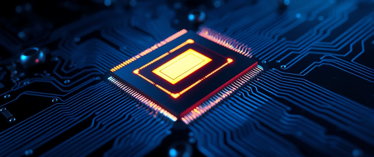
Intel 4004 (1971)
Intel Core i9-14900K (2023)
Detailed specs for each, for direct comparison:
- Transistors: 2,300
- Process node: 10 microns
- Architecture: 4-bit
- Clock speed: 740 kHz
- Price at launch: $200
- Designers: Federico Faggin, Ted Hoff, Stan Mazor
Intel Core i9-14900K (2023):



- Transistors: 6 billion
- Process node: Intel 7 (10nm equivalent)
- Architecture: 64-bit, hybrid P+E core design
- Maximum clock speed: 6.0 GHz
- Performance cores: 8, Efficiency cores: 16
- TDP: 125W base, 253W maximum turbo
From 1971 to 2023, transistor count per chip rose roughly 2.6 million times, and clock speed climbed from 740 kHz to 6.0 GHz – a factor of about 8,108x. See CPU generations explained for how this scaling continues today.
Moore’s Law: Accuracy and Limits
Moore’s Law says transistor count on a chip doubles about every 2 years. Gordon Moore stated it in 1965 from 1959-1965 data. It held for decades, then slowed:
- 1965–2000: held closely, doubling period averaged 1.9 years
- 2000–2015: held approximately, doubling period averaged 2.5 years
- 2015–2024: slowing significantly, density improvements dropped to 10–15% per generation vs. 50%+ historically
Generation 5: AI and Parallel Computing Hardware (2010s-Present)
Fifth-generation computing uses massively parallel architectures and AI-specialized silicon. The NVIDIA H100 GPU (2022) exemplifies it:
- Transistors: 80 billion
- Process node: TSMC 4N (4nm-class)
- CUDA cores: 16,896
- FP16 performance: 3.9 petaFLOPS
- FP8 performance: 7.8 petaFLOPS (with sparsity: 15.6 PFLOPS)
- HBM3 memory: 80GB
- Memory bandwidth: 3.35 TB/s
- TDP: 700W
Key Milestones in Computer History: Year-by-Year Table
The table tracks the landmark machines and their defining specifications across all five generations:
| Year | Milestone | Key Specification |
|---|---|---|
| 1945 | ENIAC operational | 17,468 vacuum tubes, 5,000 additions/sec |
| 1951 | UNIVAC I, first commercial computer | Delivered to U.S. Census Bureau |
| 1958 | First integrated circuit | Jack Kilby, Texas Instruments |
| 1964 | IBM System/360 | First compatible software family |
| 1971 | Intel 4004 microprocessor | 2,300 transistors, 740 kHz, 4-bit |
| 1975 | Altair 8800 personal computer kit | $439, Intel 8080, hobbyist market |
| 1981 | IBM PC | Intel 8088, 16KB RAM, open architecture |
| 1991 | World Wide Web | Tim Berners-Lee, HTTP/HTML |
| 1993 | Intel Pentium | 60 MHz, 3.1 million transistors |
| 2006 | Intel Core 2 Duo, multi-core mainstream | 2 cores, 65nm, 2.4 GHz |
| 2022 | NVIDIA H100 GPU | 80 billion transistors, 3.9 petaFLOPS FP16 |
| 2023 | Intel Core i9-14900K | 6 billion transistors, 6.0 GHz max boost |
Transistor Scaling: From 10 Microns to 3 Nanometers
Feature size shrank from 10,000 nm (Intel 4004, 1971) to 3 nm (Apple M3 / TSMC N3, 2023) – about a 3,333x reduction in linear dimension and roughly an 11-million-times rise in density per unit area:
- TSMC N3E (3nm): used in Apple M3, A17 Pro, 60% higher transistor density vs. N5
- Samsung 3GAE (3nm): Gate-All-Around (GAA) transistor architecture
- Intel 18A (1.8nm): expected 2025, uses RibbonFET (GAA) and PowerVia backside power delivery
Best for context: smaller nodes pack more transistors per chip at lower power, which is what keeps performance climbing as raw clock-speed gains flatten.
From General-Purpose to Domain-Specific Computing
Modern computing is splitting into general-purpose CPUs and domain-specific accelerators. CPUs handle sequential tasks; accelerators handle parallel or specialized workloads far more efficiently:
- Google TPU v5p: 459 teraFLOPS BF16 per chip, designed for large language model training
- Apple Neural Engine (M4): 38 TOPS (trillion operations per second) for on-device AI inference
- Cerebras WSE-3: 900,000 AI cores on a single wafer-scale chip, 125 petaFLOPS
- Amazon Trainium2: 2x performance per watt vs. Trainium1 for AWS cloud training
Last Thoughts on the Evolution of Computers
Computer evolution followed five hardware generations, each defined by a new switching technology. ENIAC in 1945 did 5,000 additions per second; the NVIDIA H100 in 2022 does 3.9 quadrillion FP16 operations per second – a ratio of about 780 billion to 1. The current era is defined not by transistor scaling alone, but by architectural specialization for AI workloads.
Key Takeaways:
- ENIAC (1945) used 17,468 vacuum tubes and weighed 30 tons; modern processors fit billions of transistors on a fingernail-sized chip.
- Moore’s Law held from 1965 to approximately 2015; transistor doubling now takes 3–4 years instead of 2.
- The Intel 4004 (1971) had 2,300 transistors at 10 microns; the Intel Core i9-14900K (2023) has 6 billion at 10nm.
- The NVIDIA H100 GPU delivers 3.9 petaFLOPS FP16, purpose-built for AI workloads, not general computation.
- TSMC’s 3nm process node represents a 3,333x reduction in feature size from the original 10-micron Intel 4004.
- Fifth-generation computing is defined by parallel, AI-specialized architectures rather than sequential, general-purpose CPUs.
Frequently Asked Questions (FAQs)
What generation of computers are we in now?
Computing is in the fifth generation, characterized by AI-specialized hardware, massively parallel processing, and domain-specific chips like GPUs, TPUs, and neural processing units introduced from the 2010s onward.
How many transistors did ENIAC have?
ENIAC used 17,468 vacuum tubes, not transistors. The transistor was not yet invented. ENIAC was completed in 1945 and weighed 30 tons.
What replaced vacuum tubes in second-generation computers?
Transistors replaced vacuum tubes. The transistor was invented at Bell Labs in 1947 and appeared in commercial computers by the late 1950s, reducing size by 50x and improving reliability substantially.
When did microprocessors first appear?
The first commercial microprocessor, the Intel 4004, was released on November 15, 1971. It contained 2,300 transistors on a 10-micron process and ran at 740 kHz.
Is Moore’s Law still valid?
Moore’s Law is slowing. From 1965–2015 transistor counts doubled roughly every 2 years. Since 2015 density improvements dropped to 10–15% per generation, and the doubling period is now 3–4 years.
About the author

Nizam Ud DeenFounder and Tech Blogger
Muhammad Nizam Ud Deen Usman is the founder of theCoreiTech and the author of The Local SEO Cosmos. He has worked in search since 2014 as an SEO consultant for eCommerce stores and local businesses, specialising in eCommerce SEO, local SEO and technical SEO, and runs SEO Academy and the SEO Community from Multan, Pakistan. He also founded ORM Digital Solutions, a digital agency serving medium and large businesses, and holds a degree from the University of Education, Lahore (Multan Campus). Plerdy lists him among its Best 20+ SEO Experts in Pakistan. Nizam started theCoreiTech in 2012 to make computers easier to understand and use for everyone. More of his work is at nizamuddeen.com.
